
Search results
There is a page named "Plasmonic nanolithography" on Wikipedia
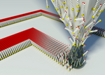
- Plasmonic nanolithography (also known as plasmonic lithography or plasmonic photolithography) is a nanolithographic process that utilizes surface plasmon...13 KB (1,200 words) - 12:57, 30 October 2023
- Yu, Weixing; Wang, Taisheng; et al. (31 May 2011). "Plasmonic nanolithography: a review". Plasmonics. 6 (3): 565–580. doi:10.1007/s11468-011-9237-0. S2CID 119720143...16 KB (1,682 words) - 09:17, 28 May 2024
- ferroelectric nanolithography. Compared to conventional photoexcitation, the material produced three to 10 times the current. In the past 5 years plasmonic nanoparticles...15 KB (1,875 words) - 00:42, 26 June 2024
- Yu, Weixing; Wang, Taisheng; et al. (31 May 2011). "Plasmonic nanolithography: a review". Plasmonics. 6 (3): 565–580. doi:10.1007/s11468-011-9237-0. S2CID 119720143...16 KB (1,991 words) - 03:23, 16 May 2024
- Cheng; Bogy, David B.; Zhang, Xiang (2008). "Plasmonic lens in the near field for high-speed nanolithography" (Free PDF download). Nature Nanotechnology...6 KB (599 words) - 19:17, 26 July 2024
- doi:10.1109/PROC.1974.9627. Srituravanich, W.; et al. (2004). "Plasmonic Nanolithography" (PDF). Nano Letters. 4 (6): 1085–1088. Bibcode:2004NanoL...4...97 KB (11,286 words) - 04:47, 13 July 2024
 Dip pen nanolithography (DPN) is a scanning probe lithography technique where an atomic force microscope (AFM) tip is used to directly create patterns...22 KB (2,562 words) - 18:44, 6 June 2024
- Werayut; Fang, Nicholas; Sun, Cheng; Luo, Qi; Zhang, Xiang (2004). "Plasmonic Nanolithography". Nano Letters. 4 (6). American Chemical Society (ACS): 1085–1088...15 KB (1,938 words) - 02:54, 6 June 2024
 Nanochemistry (section Nanolithography)Light coupling nanolithography Scanning probe microscope Nanoimprint lithography Dip-Pen nanolithography Soft lithography Each nanolithography technique has...38 KB (4,397 words) - 00:12, 10 June 2024
 attention in recent years deals with one- and two-dimensional (1D and 2D) plasmonic arrays with subwavelength periodicity, also known as metasurfaces. Due...28 KB (2,925 words) - 18:20, 13 August 2024
- Plasmonic cover, Theories of cloaking Plasmonic laser, Nanolaser Plasmonic metamaterials Plasmonic nanolithography Plasmonic Nanoparticles Plasmonic solar...24 KB (195 words) - 20:51, 11 August 2024
 is a method of fabricating nanometer-scale patterns. It is a simple nanolithography process with low cost, high throughput and high resolution. It creates...33 KB (3,940 words) - 22:10, 16 May 2024
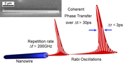 Stefan A.; Ronning, Carsten; Oulton, Rupert F. (2014-09-28). "Ultrafast plasmonic nanowire lasers near the surface plasmon frequency". Nature Physics. 10...5 KB (527 words) - 15:48, 6 December 2023
- than the wavelength—for example, drawing 30 nm lines using 193 nm light. Plasmonic techniques have also been proposed for this application. Heat-assisted...24 KB (2,690 words) - 04:30, 31 July 2024
 have reached scales below 100 nanometers, using electron beam and nanolithography. One nanoscale SRR cell has three small metallic rods that are physically...45 KB (4,373 words) - 22:07, 18 May 2024
- working on research topics such as nanophotonics, optical nanolithography, superlenses, and plasmonics. For his postgraduate work, Balzarotti relocated to Germany...9 KB (702 words) - 20:42, 5 June 2024
 53rd International Symposium on Electron, Ion, and Photon Beams and Nanolithography, Marco Island, FL, May 26–29, 2009. Duan, Huigao; Winston, Donald;...65 KB (7,214 words) - 04:28, 31 July 2024
 doi:10.1070/PU1968v010n04ABEH003699. "Three-Dimensional Plasmonic Metamaterials". Plasmonic metamaterial research. National Institute of Standards and...72 KB (7,633 words) - 05:58, 10 June 2024
- determined as the sensor signal. Other examples include electromagnetic or plasmonic nanosensors, spectroscopic nanosensors such as surface-enhanced Raman...50 KB (6,123 words) - 08:02, 6 June 2024


- much higher than the bass. The bass can only be heard in the near field. plasmonics Rochester Nano Optics Lucas Novotny and Bert Hect, Principles of Nano-Optics