
Search results
There is a page named "Multiple layered plasmonics" on Wikipedia
- Multiple layered plasmonics use electronically responsive media to change and manipulate the plasmonic properties of plasmons. The properties typically...7 KB (826 words) - 11:27, 6 April 2024
 Multiple patterning (or multi-patterning) is a class of technologies for manufacturing integrated circuits (ICs), developed for photolithography to enhance...65 KB (7,214 words) - 04:28, 31 July 2024
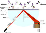
- A plasmonic-enhanced solar cell, commonly referred to simply as plasmonic solar cell, is a type of solar cell (including thin-film or wafer-based cells)...47 KB (6,109 words) - 21:19, 20 August 2024
- techniques and infrared spectroscopy. Potential applications of graphene plasmonics involve terahertz to midinfrared frequencies, in devices such as optical...24 KB (2,615 words) - 06:08, 30 June 2024
 Surface plasmon resonance (category Plasmonics)S2CID 252548497. Maradudin AA, Sambles JR, Barnes WL, eds. (2014). Modern Plasmonics. Amsterdam: Elsevier. pp. 1–23. ISBN 9780444595263. Bakhtiar, Ray. "Surface...30 KB (3,653 words) - 04:42, 22 August 2024
 A nanoscale plasmonic motor (sometimes called a "light mill") is a type of nanomotor, converting light energy to rotational motion at nanoscale. It is...14 KB (1,772 words) - 21:33, 31 July 2022
 Surface plasmon polariton (category Plasmonics)the performance of plasmonic devices. The need for lower loss has fueled research aimed at developing new materials for plasmonics and optimizing the...39 KB (5,101 words) - 20:23, 15 August 2024
 Photonic metamaterial (category CS1 maint: multiple names: authors list)mirror to work.) The material combined two optical nanostructures: a multi-layered block of alternating silver and glass sheets and metal grates. The silver-glass...45 KB (4,373 words) - 22:07, 18 May 2024
- Codes for electromagnetic scattering by spheres (section Codes for electromagnetic scattering by a layered sphere)article list codes for electromagnetic scattering by a homogeneous sphere, layered sphere, and cluster of spheres. Majority of existing codes for calculation...13 KB (774 words) - 00:20, 21 January 2024
- Materials today. He holds multiple patents. Moreover, he is the recipient of 2016 Facebook Academy Award for his work on plasmonics. Rivas earned his Master's...13 KB (1,372 words) - 19:44, 10 July 2024
 semiconductors. Cells made from multiple materials layers can have multiple bandgaps and will therefore respond to multiple light wavelengths, capturing...61 KB (8,208 words) - 17:15, 22 July 2024
- out-phase mode coupling between graphene plasmonics and metal plasmonics is realized. The tunable properties of the plasmonic metal-graphene nanoantenna can be...136 KB (15,287 words) - 04:41, 31 July 2024
- photomask in direct contact with a substrate coated with an imaging photoresist layer. The first integrated circuits had features of 200 micrometres which were...15 KB (1,938 words) - 02:54, 6 June 2024
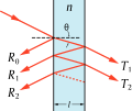
 Total internal reflection in prisms finds numerous uses through optics, plasmonics and microscopy. In particular: Prisms are used to couple propagating light...14 KB (1,727 words) - 15:01, 19 August 2024
 Metamaterial (category CS1 maint: multiple names: authors list)Ari Sihvola; Alexey P. Vinogradov (December 2008). Metamaterials and Plasmonics: Fundamentals, Modelling, Applications. New York: Springer-Verlag. pp...92 KB (9,946 words) - 18:13, 14 August 2024
- V–VI semiconductors II–V semiconductors I–III–VI2 semiconductors Oxides Layered semiconductors Magnetic semiconductors Organic semiconductors Charge-transfer...54 KB (2,517 words) - 22:57, 26 August 2024
 reflection probabilities from a multilayer with complex indices of refraction. Layered Materials and Photonic Band Diagrams (Lecture 23) in MIT Open Course Electronic...14 KB (2,216 words) - 09:57, 18 August 2024
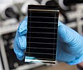 organic–inorganic lead or tin halide-based material as the light-harvesting active layer. Perovskite materials, such as methylammonium lead halides and all-inorganic...186 KB (21,033 words) - 21:12, 16 August 2024
 Thin-film solar cell (category Pages using multiple image with auto scaled images)roughening of the photovoltaic layers (thereby preventing increase of recombination). Besides surface texturing, the plasmonic light-trapping scheme attracted...127 KB (14,324 words) - 16:56, 14 July 2024
- Electrochromic device (category CS1 maint: multiple names: authors list)there are three principally different kinds of layered materials in the ECD: The EC layer and ion-storage layer conduct ions and electrons and belong to the...13 KB (1,722 words) - 00:24, 16 December 2023


- near-IR region of the spectrum between 700 and 900 nm. Small quantities of plasmonic Ag and Au particles also make brightly colored and strongly scattering