
Search results
There is a page named "Electron beam induced deposition" on Wikipedia
- Electron-beam-induced deposition (EBID) is a process of decomposing gaseous molecules by an electron beam leading to deposition of non-volatile fragments...12 KB (1,419 words) - 20:16, 10 December 2023
- Chemical vapor deposition, a chemical process used in the semiconductor industry to produce thin films Electron beam-induced deposition, a process of decomposing...4 KB (546 words) - 19:42, 27 August 2024
- 2014, 117, 1631–1644. "Electron Induced Surface Reactions of cis-Pt(CO)2Cl2: a Route to Focused Electron Beam Induced Deposition of Pure Pt Nanostructures...14 KB (1,488 words) - 04:11, 24 May 2023
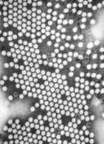 Transmission electron microscopy (TEM) is a microscopy technique in which a beam of electrons is transmitted through a specimen to form an image. The specimen...118 KB (15,058 words) - 21:08, 30 July 2024
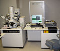 site-specific analysis, deposition, and ablation of materials. A FIB setup is a scientific instrument that resembles a scanning electron microscope (SEM). However...26 KB (3,322 words) - 22:07, 2 March 2024
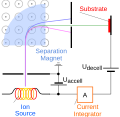 Ion beam deposition (IBD) is a process of applying materials to a target through the application of an ion beam. An ion beam deposition apparatus typically...6 KB (689 words) - 13:45, 25 August 2024
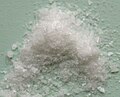 carbonyl is widely used in electron beam-induced deposition technique - it is easily vaporized and decomposed by the electron beam providing a convenient...7 KB (589 words) - 08:07, 5 July 2024
 hexacarbonyl is widely used in electron beam-induced deposition technique - it is easily vaporized and decomposed by the electron beam providing a convenient...12 KB (951 words) - 04:36, 15 April 2024
 Ion source (redirect from Electron beam ion source)by the electron beam ion trap. Electron capture ionization (ECI) is the ionization of a gas phase atom or molecule by attachment of an electron to create...58 KB (7,140 words) - 08:46, 21 February 2024
 electron microscope (SEM) is a type of electron microscope that produces images of a sample by scanning the surface with a focused beam of electrons....67 KB (8,141 words) - 10:21, 21 August 2024
 Electron-beam lithography (often abbreviated as e-beam lithography or EBL) is the practice of scanning a focused beam of electrons to draw custom shapes...38 KB (4,736 words) - 09:02, 10 July 2024
 Catalyst nanoparticles. Electron beam induced deposition – a technique of growing nanostructures and nanodevices using the beam of electron microscope. Besides...15 KB (1,612 words) - 13:23, 2 December 2023
- Field electron emission, also known as field emission (FE) and electron field emission, is emission of electrons induced by an electrostatic field. The...125 KB (16,087 words) - 09:14, 8 February 2024
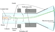 Cathode-ray tube (section Electron gun)cathode-ray tube (CRT) is a vacuum tube containing one or more electron guns, which emit electron beams that are manipulated to display images on a phosphorescent...265 KB (28,861 words) - 07:30, 28 August 2024
 3D printing processes (redirect from Direct Metal/Material Deposition)surrounding the laser), or in a sealed chamber. Electron beam freeform fabrication uses an electron beam heat source inside a vacuum chamber. It is also...74 KB (8,099 words) - 21:43, 22 August 2024
 hundred nanometers negative. Electron beam induced deposition Electron diffraction Electron energy loss spectroscopy (EELS) Electron microscope Energy filtered...19 KB (2,788 words) - 14:01, 7 August 2024
- EBID may refer to: Electron beam-induced deposition, a nanoscale deposition technique Evidence-based individual decision making, see Evidence-based medicine...189 bytes (52 words) - 02:35, 10 February 2024
 PMID 19498166. S2CID 3731481. Donev, E.U.; Hastings, J.T. (2009). "Electron-Beam-Induced Deposition of Platinum from a Liquid Precursor". Nano Letters. 9 (7):...16 KB (1,709 words) - 18:14, 2 August 2023
 fastest deposition rates while maintaining film quality (such as roughness, defects/voids), as compared with sputter deposition and thermal/electron-beam evaporation...12 KB (1,474 words) - 22:58, 4 June 2024
 low-light camera. In the microscope an incident beam of electrons hits a tilted sample. As backscattered electrons leave the sample, they interact with the atoms...124 KB (13,682 words) - 20:39, 19 July 2024


- space environment, combined with anticipated advances in laser-, electron-, and ion-beam technologies, may make possible automated machinery capable of
- Focused, Nanoscale Electron-Beam-Induced Deposition and Etching by Randolph et al. [http://www.febip.info/ Focused Electron Beam Induced Processes (FEBIP)]